PCB MANUFACTURING


EXPERIENCE AND RELIABILITY

Many years of cooperation with a number of approved PCB manufacturers. Regular audits of manufacturers. The ability to choose the best manufacturer based on the project specifications.

ENGINEERING SUPPORT

Support of each order by an appointed IKT engineer who verifies, checks for compliance with IPC standards and adapts the customer’s design documentation for production, as well as advises the customer on PCB design and its optimization.

input and output control

Quality control of printed circuit boards is carried out in accordance with the requirements of IPC-A-600 Standard. At customer’s request, additional printed circuit board’s parameters tests are possible.

PRICE OPTIMIZATION

Flexibility in optimizing prices, based on the technological capabilities of manufacturers and logistic options.

Product range

Multilayer PCBs

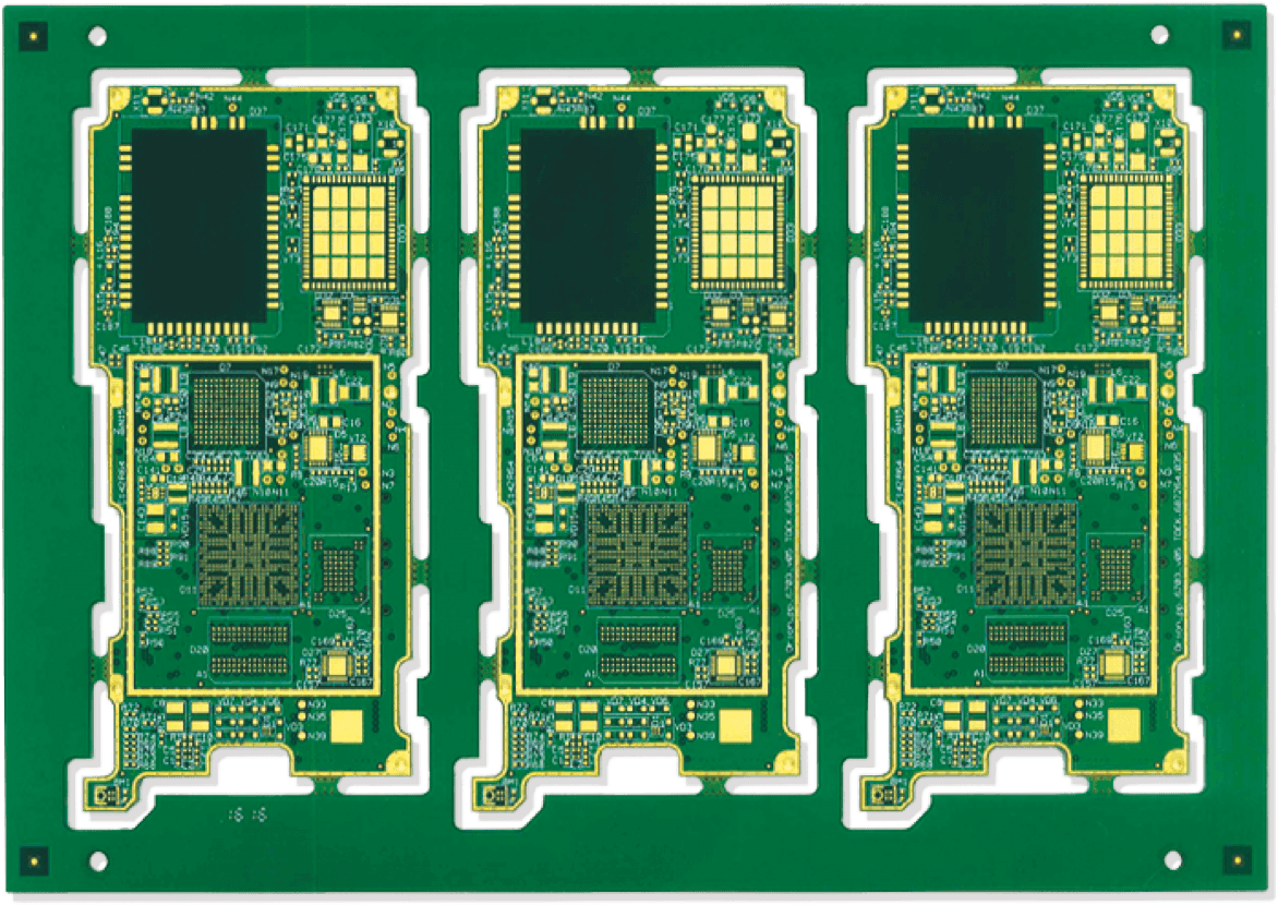
A wide range of dielectrics with various parameters are used to manufacture ML printed circuit boards. The most advanced materials (enhanced FR4, FR4 High Tg) allow producing boards with big layer quantity and complex route patterns.

Microvave PCBs

A distinctive feature of microwave printed circuit boards is a wide range of high-frequency signals that are distributed through strip lines of transmissions. This fact is reflected in the special features of design of the microwave circuit boards and sets up special demands for the parameters of dielectrics and the quality of manufacture of the print pattern elements. In the manufacture of microwave printed circuit boards high-frequency laminates are used. These materials are reinforced by glass fiber polymer and ceramic thermoset laminates with a little tangent of an angle of dielectric losses and a wide range of dielectric coefficient.

Flexible, rigid-flexible PSBs

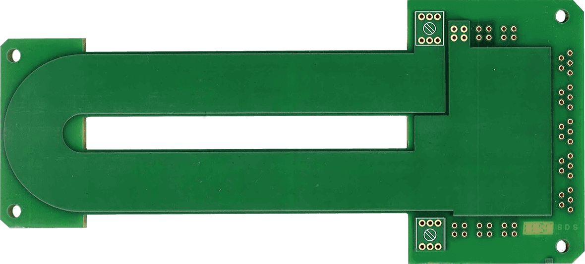
Flexible circuit boards (up to 8 layers) and flat flexible cables have significantly advantages over traditional wired cables in complex devices, reducing assembling cost and allowing to connect different connectors and components in different locations in 3D designs. The core materials are low thickness polyimide films and PET.

Metal core PCBs

The main feature of metal core printed circuit boards is thick metal plate (such as Al, Cu, Fe) and thin dielectric with high thermal conductivity thus allowing to increase overall heat dissipation and easily attach board to heat sink.

HDI Multilayer PCBs

The highest quality basic materials, sophisticated manufacturing processes and most advanced technologies are used for HDI printed circuit boards production. HDI PCB design has buried vias, blind laser micro vias, conductors width and gaps under 100 um.

Impedance Controlled PCBs

Impedance controlled printed circuit boards are manufactured of materials with high stable parameters. A special attention is paid to the board’s stack up, route patterns of transmission lines. It allows to minimize the signal losses and provide high speed data transmission.

Backplane PCBs

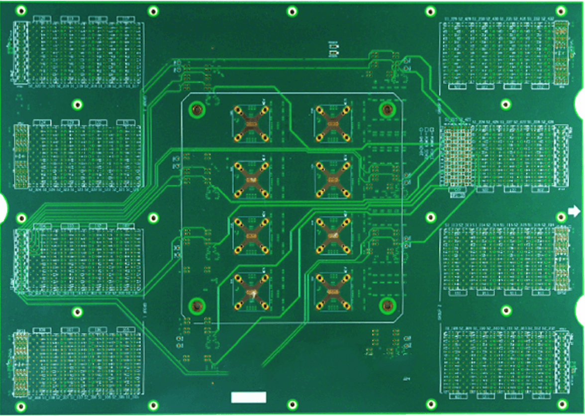
Backplane are big size multilayer printed circuit boards with over than 20 layers and with high thickness. Backplanes structure has thick copper foil, power bus, high speed and impedance control layers. Backplanes can have holes for press-fit connectors and special technology back drilling holes.

Planar Transformers

Using of planar transformers minimizes size of devices and improves design reliability. For manufacturing of planar transformers the dielectrics with high breakdown voltage and thick foil are used to maintain high currents and interlayer insulations.

PCBs with embedded components

PCBs with embedded components are the most complex to manufacture. Special technologies allow to include the lead free chip components, uncased transistors, diodes, etc. inside of multilayer PCBs. It is also possible to create the structure of the resistive layers which allows to form thin film resistors. The usage of embedded components can reduce the size and weight of the device, as well as increase reliability.
Delivery terms of prototypes and small batch quantities are from 1.5 weeks with urgent delivery, up to 4 weeks with regular delivery. The term of delivery of large-scale consignments by container transportation is from 2 months.

Cost of manufacture

To find out cost of manufacture , please, send the request

In the inquiry, please, specify the following parameters: PCB type, dielectric material, reliability class; PCB dimensions; Finished board thickness and tolerance Starting thickness of copper and dielectrics PCB stack-up Surface finish type Minimum track / spacing size Minimum hole size Quantity ordered

To make an order, PCB project or design documentation in Gerber format (RS-274X) and a drilling file in Excelon or HPGL format is to be provided.

CONTACTS

VICTORIA LUZAN

Head of Customer Service Department
Industrialna Street 2, Chernihiv, Ukraine, 14011

EKATERINA LADOVICH

CUSTOMER DEPARTMENT MANAGER
Industrialna Street 2, Chernihiv, Ukraine, 14011